Home »
Nanotechnology
Fundamental Networking Issues in CANETS
By Vandana Sharma, on July 24, 2017
In this section we consider an application example of CANETs, i.e., a nanoscale biosensor net-work (NBSN) to detect hazardous antigen concentration as an immune system support, and then highlight the corresponding networking challenges and open issues to be addressed. In addition to the hardware components given earlier, we assume that nanonodes in NBSNs also have a sensing unit to detect the presence of antigen molecules.
Deployment
There is necessity of the dense deployment of nanonodes for network-wide connectivity with smaller energy consumption.
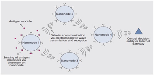
Figure: Illustration of a CANET Application Example, i.e., Nanoscale Bio-Sensor Network [Atakan Baris and Ozgur B. Akan ,2010,”Carbon Nanotube-Based Nanoscale Ad Hoc Networks,” IEEE Communication Magazine, Vol 6804]
Multi-hop Reliability
Upon the transmission of the information signal, additional functionalities and challenges should be overcome to route the signal among CANET nodes. A possible routing scheme may be similar to flooding-based routing mechanisms if CNT receivers and transmitters are used in nanotransceiver circuitry since they naively generate analog signals that radiate along the network. However, CNT antennas provide the capability of directivity for nanonode transmission However, power consumption required by data storage and computation may seriously reduce network lifetime. Therefore, an efficient store-and-forward scheme should also take into account the power consumption required by data storage and computation.
Medium Access Control
Correspondingly, due to their high computation complexity requirement, CDMA mechanism may also not be correct for the configuration with CNT antennas. Instead, a much simpler form of frequency-division multiple access based or time-division multiple access (TDMA)-based approaches might be suitable to efficiently access the communication medium. The realization of such an access mechanism clearly entails the efficient selection of transmission frequencies.
Performance Analysis
In this topic, an analysis on scaling is done. Different parameters are compared for different scaling values.MOS Transistor Scaling is done by scaling transistor horizontal dimensions, vertical dimensions and operating voltage, simultaneous improvements in transistor density, switching speed and switching energy can be realized.
For ideal scaling, a 0.7 reduction in MOS transistor dimensions and operating voltage, along with an increase in silicon dopant concentration, will provide transistors with the following improvements: 2 areal density, 0.7 switching delay time and 0.5 switching energy. This is summarized in the table below.
Table - Ideal Scaling Improvements
| Ideal Scaling |
| Arial Density |
Switching Delay Time |
Switching Energy |
| 2 folds |
0.7 folds |
0.5 folds |
Table - NMOS Transistor Characteristics for 0.5µm AND 0.13µm Generations of Logic Technology
| Technology Generation |
0.5 µm |
0.13 µm |
22nm |
| Early Manufacturing |
1992 |
2001 |
2014 |
| Supply Voltage(VDD),in V |
3.3 |
1.2 |
0.7 |
| Gate Length(LG),in µm |
0.50 |
0.07 |
0.01 |
| Physical Gate Oxide (TOXP),nm |
10.5 |
1.8 |
Hi-k |
| Electrical Gate Oxide(TOXE),nm |
11.0 |
2.6 |
0.8 |
| Drive Current(I DSat),mA/µm |
0.4 |
0.8 |
1.0 |
| Off Current(I OFF), nA/µm |
<0.1 |
10 |
500 |
| Gate Delay(CV/I),Ps |
13 |
1.4 |
0.3 |
| Switching Energy(CV2),J |
8.5 |
0.17 |
0.005 |
Table summarizes typical NMOS transistor characteristics for the older 0.5µm generation and today's 0.13µ m generation. Note that L values, which used to be the same as other typical feature sizes on a generation, are now almost half the typical feature size. L dimensions have been scaling faster than other feature sizes in order to accelerate MOSFET performance improvements, and, therefore, accelerate product performance improvements. Transistor gate delay has reduced by almost an order of magnitude and switching energy has improved by a factor of 50 between 0.5µ m and 0.13µm generations (assuming W m and 0.13µm for each respective generation).
The even smaller devices plotted suggest that scaled MOS transistors will continue to provide predictable improvements in delay and energy for some time to come. However, there are emerging signs that MOS transistors are reaching their scaling limit. Scaled MOS transistors require reduced threshold voltage (V) that leads to higher subthreshold leakage current (I). As shown in Table , typical 0.13 m generation transistors have I values of 10 nA/ m, more than a 100 increase over 0.5µ m generation transistors. This trend may be obvious for MOS technology as indicated by all the sub-40 nm transistor publications having I values of 100 nA/ m or more. It is doubtful whether future microprocessors with a billion transistors can tolerate leakage values of more than a few hundred nA/ m due to standby power limitations. Another limiter to MOSFET scaling is gate oxide scaling.
Today's 0.13µm technologies use SiO gate dielectrics as thin as 1.5 nm, less than seven atomic layers thick. Gate oxide leakage is increasing exponentially with each new generation due to oxide thickness scaling and is beginning to approach transistor subthreshold leakage values (1 nA/ m). To address this limitation, a significant amount of research is underway on high- gate dielectrics to replace SiO. The controllability of MOSFET device characteristics at very small dimensions will become an issue due both to lithography variation and arbitrary dopant fluctuation in channel regions affecting V control. Despite these serious scaling concerns, novel 3-dimensional double gate transistor structures are rising that could push MOS technology beyond restrictions foreseen for traditional planar bulk CMOS.
Table - Semiconductor Memory Attributes
| Memory Technology
| DRAM |
SRAM |
NOR Flash |
NAND Flash |
| Cell Size (General) |
8 F2 |
130 F2 |
10 F2 |
7 F2 |
| Cell Size (0.13 µm) |
0.14µm2 |
2.20 µm2 |
0.17 µm2 |
0.12 µm2 |
| Access Time |
<50 ns |
<5 ns |
<100 ns |
-2 µs |
| Program/Erase |
<50 ns |
<5 ns |
1 µs/500ms |
10 ms/10ms |
| P/E Cycle Endurance |
>1013 |
>1013 |
>105 |
>105 |
| Refresh Needed? |
Yes |
No |
No |
No |
| Volatile |
Yes |
Yes |
No |
No |
In memory applications as shown in Table DRAM has a small cell size and reasonable access time, but will lose its stored information when the power supply is removed (a volatile memory) and will also lose charge during normal operation due to cell leakage, thus, the information in each cell must be refreshed more than once per second. SRAM has the fastest access time and does not require refresh, but is volatile and has the largest cell size. Flash memory has a small cell size, is nonvolatile and does not require refresh, but access time is slow, program/erase time is very slow and the cell wears out after 10 –10 program/erase cycles threshold voltage ( 0.5 V). The leakage requirements for DRAM transistors are much more stringent than for logic transistors. As a result, DRAM transistors have not scaled as fast as logic transistors and generally have longer channel lengths, thicker gate oxides and higher operating voltages. During DRAM operation, charge stored on C is dumped onto a bit line by turning on the access transistor .A comparison between DRAM, SRAM, NOR Flash and NAND Flash, depending upon the cell size, access time, program/erase time and requirement of refresh and volatility is illustrated in Table.
Advertisement
Advertisement