Home »
Nanotechnology
Nanotechnology - Graphene and It's properties
By Vandana Sharma, on July 01, 2017
What is Graphene in Nanotechnology?
Graphene which is a one-atom-thick layer of carbon atoms, has recently attracted great interest among physicists and engineers. The carbon atoms arearranged in a honeycomb lattice. The amalgamation of the exceptional properties of graphene with innovative device concept and nanotechnology can overcome some of the main problems of traditional radio frequency electronics in terms of maximum frequency, linearity, and power dissipation. In this article we review the current status of research on graphene based electronic devices for RF applications. The future challenges facing this rising technology and its feasibility for a new generation of applications in RF communications and circuits are also discussed.
Overview of Graphene
Graphene was isolated in 2004 by scientists from the University of Manchester and it was the great effort made in order to extract or isolate graphene which is a one-atom-thick layer of carbon atoms arranged in a honeycomb lattice through sp2 bonding. Considered for many years an impossible goal, the isolation of graphene triggered a revolution not only among condensed matter physicists but also among chemists and engineers, eager to take advantage of its unique properties.
Graphene Properties
Graphene has unique transport properties due to the symmetry of its honeycomb lattice structure. For example, the carriers in graphene lose their effective mass and can be described by a Dirac-like equation instead of by the Schrödinger equation used in traditionalsemiconductors. This very low effective mass is responsible for a very high electron and hole mobility in excess of 200,000 cm2/Vs at T= 5 K and in excess of 100,000 cm2/Vs at T= 240 K in suspended graphene, the highest ever reported for any semiconductor.
Graphene has zero-bandgapas the conduction and valence bands in this material, touch one another at a point called the Dirac point. In addition to this zero bandgap, the density of states in graphene is zero at the Dirac point and increases linearly for energies above and below it, which allows for carrier modulation. The charge carriers are confined to one atom thick layer only. This allows unprecedented electrostatic confinement, and also makes graphene extremely flexible and transparent. These unique properties of graphene have motivated intense work among physicists and engineers who have seen in this material new opportunities to improve digital and RF electronics, advanced sensors, transparent electronics, low-power switches, solar cells, and even battery energy storage. In this article some of the recent progress made in the use of graphene devices for communication applications are reviewed. The next section discusses the various growth techniques currently used to synthesize graphene, and then the basic fabrication technology common to many graphene devices is introduced. Then several graphene devices with the potential to impact future communication systems are described. So graphene is grabbing importance in applications like low noise amplifiers, nonlinear electronics, in RF electromechanical resonators and switches.
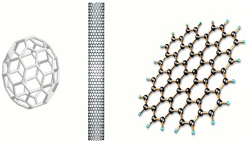
Diagram of Different Low-Dimensional Carbon Structures
[Refer: UdoSchwalke, 2008,” Nanotechnology: The Power of small”, International Conference on signals, circuits and systems.]
Graphene was first discovered through the successive peeling of highly HOPG using scotch tape 1. This amazingly simple method, also known as mechanical exfoliation, has been effective at producing graphene flakes 20–1000 µ m in length,and has been the primary source material for most papers reporting graphene’s extraordinary physical and electronic properties. Unfortunately, while these flakes have generated impressive performance, working with them involves consuming effort to locate and identify single-layer flakes. Furthermore, electron beam lithography is necessary to pattern graphene transistors in these randomly arranged flakes, and it usually has a throughput of only a couple of transistors per sample.
Reference: Graphene
Advertisement
Advertisement