Home »
Nanotechnology
Graphene Fabricated Devices
By Vandana Sharma, on July 04, 2017
Graphene Fabricated Devices
Although graphene shares many of its outstanding properties with carbon nanotubes, graphene devices are strongly preferred from a commercial point of view because their fabrication is very similar to traditional planar wafer-size Si processing. Devices are patterned using standard photolithography tools or electron-beam lithography. Metal contacts are deposited through lift off, and graphene is subsequently etched with oxygen plasma. Finally, a gate dielectric is deposited and the gate metal is patterned. Most of the fabrication technology mirror all the work done on carbon nanotube field effect transistors (CNT-FETs) in terms of selection of ohmic metals, gate dielectrics, and so on. Every atom in a graphene film is at the surface and strongly interacts with the surrounding environment, which opens numerous opportunities for new device concepts, but also new sources of performance degradation. So far the most dominant mechanism for mobility degradation in graphene is charged impurities.
Therefore, much work has been dedicated to studying various high-k dielectric materials and substrates to screen the effects of any charged impurities and reduce surface phonon effects. In spite of some partial success in identifying suitable substrates, more work is needed in this area as the reported nobilities are still far from the record mobility recorded in suspended graphene, where the substrate underneath the graphene film was etched away. The lack of substrate in these measurements prevents any degradation through surface vibrations (phonons) or nearby charged impurities, both of which greatly reduce graphene’s intrinsic properties. However, most practical applications require that a substrate allows for proper heat dissipation. Therefore, the choice of substrate and its interaction with graphene is of utmost importance.
A second important processing issue in graphene devices is to optimize the metallization for reducing contact resistances. Most work has been done on matching work functions of graphite and the metal. The most common metal combinations are Cr/Au, Ti/Pt, and Ti/Pd/Au. Based on experiments done in our laboratory, Cr/Au contacts give contact resistances in the range 1*〖10〗^(-4)-2*ohm.cm^2 Ti/Pt gives similar contact resistance as Cr/Au contacts. Ti/Pd/Au contacts give contact resistances in the range0.5×〖10〗^(-4)-1×〖10〗^(-4) ohm.cm^2 . However, there is still no consensus as to which one provides the lowest contact resistance. Furthermore, since graphene is so easily doped by its environment, metal on graphene may end up doping the underlying graphene, creating a potential barrier into the undoped graphene channel. This increased resistance is detrimental towards high speed operation due to the increased RC time to charge and discharge all of the capacitances ALD is the most commonly used deposition method due to the accurate control of the layer thickness that it allows. Unfortunately, ALD relies upon alternating pulses of water and precursor materials.
Graphene is hydrophobic and thus the deposition of high quality pinhole-free ALD is very difficult. Various approaches have been attempted utilizing chemical functionalization with NO2, aluminum oxidation, or seed layers to provide a template for ALD that does not reduce the mobility of the carriers in graphene. Recently, impressive results in mobility have been demonstrated through non-covalent bonding of polymers on graphene to serve as a thin buffered layer .Finally, there is growing interest in bandgap engineering of graphene. Unlike conventional semiconductors such as silicon, which contain a bandgap, graphene is a zero-bandgap material and has ON/OFF ratios around 5–10, thus limiting its effectiveness for digital applications. Much work has been focused on generating a bandgap of up to 500 meV through 1-D quantum confinement of GNR or through strain induced substrate interactions. So far, GNR have demonstrated moderate band gaps that have translated to much higher ON/OFF ratios, however the fabrication of these GNR transistors is very challenging. Electron-beam lithography is limited to feature sizes around 10–20 nm. However, to generate an appropriate sized band gap requires dimensions on the order of <10 nm. Furthermore, sidewall roughness also limits the mobility of these transistors due to edge state scattering. Another way to widen the bandgap is to apply vertical electric fields in bilayer graphene. Although this method has been successful in opening optical bandgaps (100–200meV), the electrical bandgap has been much smaller than expected (<20 meV) and more work is needed to understand the full potential of this technology.
Graphene Based Devices
1. Low Noise Amplifiers
Graphene is extremely perfect material for making high frequency low noise amplifiers. It’s extremely high mobility offers the potential of ultra low source-to-drain resistances, extremely high current densities, and high efficiency operation.
The first graphene FET (GFET), was fabricated on an HOPG graphene flake deposited on top of a SiO2/ Si substrate in 2004. The 300 nm thick SiO2 layer deposited between the Si wafer and the graphene layer serves two different functions. First, its thickness was optimized to maximize the optical contrast between the graphene flake and the substrate in order to see the flake. Second, the SiO2 layer served as gate dielectric. However, due to the large thickness of the SiO2 layer, the device transconductance was very low, severely degrading the device properties. Lemme demonstrated in 2007 the first top-gated graphene transistor. In this device, a thin SiO2 layer was used as gate dielectric. The last few years have seen a fast increase in the frequency performance of graphene transistors. Y.M Lin from IBM reported non-self aligned devices fabricated on graphene flakes with an intrinsic 100 GHz .To reduce the access resistances in these non-self-aligned devices, a substrate voltage was applied to induce carriers in the access regions.
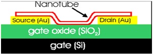
Nanotube FET [Udo Schwalke, 2008," Nanotechnology: The Power of small", International Conference on signals, circuits and systems.]
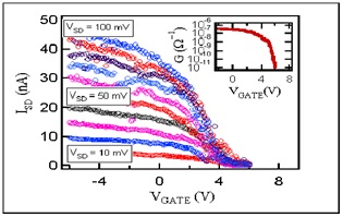
Output Characteristics of FET [Udo Schwalke, 2008,"Nanotechnology: The Power of small", International Conference on signals, circuits and systems]
To improve the ON-OFF ratio and to increase the efficiency of future graphene amplifiers, several groups are trying to induce a bandgap in graphene as discussed in the previous section. However, each of the existing methods has their limitations either in fabrication or due to edge roughness of nanoribbons.
2. Ambipolar Non Linear Electronics
One of the most intriguing properties of graphene is its ambipolar transport. In graphene ambipolar transistors, the drain current is based on hole conduction for gate-to- source voltages below the minimum conduction point voltage (VG, min) ,while at higher voltages electron conduction dominates. The V shaped current-voltage (I-V) transfer characteristic of graphene ambipolar transistors closely resembles that of an ideal full wave rectifier .With a single graphene device it is therefore possible to realize graphene device it is therefore possible to realize voltage, something that would require a full bridge circuit with four diodes made of conventional semiconductors or an operational amplifier for zero-volt rectification. Graphene ambipolar transistors can be utilized for doubling the frequency, by biasing the gate to the minimum conduction point and superimposing a sinusoidal input signal to the gate. Electrons and holes conduct in alternative half cycles to produce an output signal at the drain, whose fundamental frequency is twice that of the input. The experimental demonstration of this concept based on CVD grown graphene with an input frequency of 20 MHz and an output frequency of 40 MHz. This frequency doubler device shows high spectral purity in the output RF signal, where 93 percent of the output RF energy is at the fundamental frequency (40 MHz). This is the first time frequency doubling is realized with just a single transistor device and with high spectral purity at the output without any filtering elements. GFETs can also act as a nonlinear component for frequency mixing. The symmetrical transfer characteristics of GFETs usually show a very significant quadratic component hence, these devices can be used as excellent RF mixers. In addition, ambipolar devices can significantly reduce the number of transistors needed in these applications. Simpler circuits mean less power consumption and smaller chip area. In addition, graphene is also an ideal material for flexible electronics. Graphene grown by CVD can be transferred to arbitrary substrates, including transparent and elastic substrates. Furthermore, the two-dimensional geometry, in combination with the excellent chemical and thermal stability of graphene make fabrication of graphene circuits fully compatible and integrable with silicon technology, which is the mainstream of the semi conductor industry.
To achieve the expected high frequency performance, the device geometries and technology need to be optimized. The current frequency performance of graphene mixers is limited to tens of megahertz in this experiment due to the parasitic capacitances and resistances.
3. Graphene Resonators and RF Switches
Numerous communication systems rely on electromechanical devices, such as filters, resonators, and RF switches. The miniaturization of these devices will strongly affect the development of future communication systems. The ultimate limit to this miniaturization is represented by graphene electromechanical devices, which are only one atom thick. In fact, its enormous stiffness and low density make graphene the ideal material for these kinds of devices. The first electromechanical devices ever demonstrated in graphene were nanomechanical resonators. In 2009 Chen et al. fabricated mono-layer graphene nanomechanical resonators with operating frequencies in the 50–80 MHz frequency range. These devices showed quality factors of ~ 1×〖10〗^(-4)at low temperatures (5 K) has been predicted that graphene’s ability to withstand ultrahigh strains, up to ~25 percent in nanoindentation experiments, will allow increasing the resonance frequency of these devices above the gigahertz range while maintaining a robust signal level. Milaninia developed a switch comprising two polycrystalline graphene films grown by CVD. The top film is pulled into contact with the bottom one by applying a voltage of 5 V between the layers, and the contact is broken after removing the voltage due to restoring mechanical forces. In the ON state, more than 7 kA/cm2 of current can flow through the switch.
Advertisement
Advertisement