Home »
Embedded Systems
Memory Organization in the 8086 Microprocessor
In this tutorial, we will learn about how the memory is organized inside the 8086 Microprocessor? We will also learn that how the 8086 microprocessor is capable of handling up to 16 bits of data at a time even though each memory location in it is byte-addressable.
By Monika Sharma Last updated : May 15, 2023
There are 20 address lines in the 8086 microprocessor. This gives us 220 different memory locations. Hence the total size is 220 Bytes (as each memory location is Byte Addressable, i.e. one byte of data can be stored at every single location), which is equal to 1MB.
Even the memory is byte-addressable, yet the 8086 microprocessor an easily handle up to 16 bits of data at a time through its 16 data lines. So, to organize the memory efficiently, the entire memory in 8086 is divided into two memory banks: odd bank and the even bank.
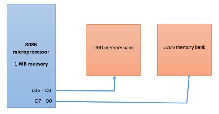
The way in which data is read or written is decided by the value of BHE, and the last address bit, that is the A0 line. It is done in the following way:
| BHE' |
A0 |
Operation performed on memory |
| 0 |
0 |
16 bits of data will be read or written into the memory |
| 0 |
1 |
8 bits of data will be read/written into the odd memory bank |
| 1 |
0 |
8 bits of data will be read/written into the even memory bank |
| 1 |
1 |
No operation is performed |
To read or write 8 bits of data, it would require only 1 CPU cycle, no matter the data is stored in any of the memory banks, but to read or write 16 bits of data, the BIU of the 8086 may require either 1 or 2 memory cycles depending upon whether the lower byte of word is located at even or odd memory address.
- If the lower byte of the word is stored at even memory bank and the upper byte is stored at odd memory bank then the CPU will require only 1 memory cycle. So, it is better to store data in this way.
- If the lower byte of the word is located at an odd memory address, then the CPU will require 2 memory cycles. The first memory cycle is required for accessing the lower byte of the word through the higher data bus, i.e. D15 to D8, and the second memory cycle is required for accessing the upper byte of the word through the lower data bus, i.e. D7 to D0.