Home »
Embedded Systems
8085 Microprocessor Architecture & Its Functional Units
In this tutorial, we will learn about the 8085 microprocessor's architecture, and its functional units in detail.
By IncludeHelp Last updated : May 13, 2023
Introduction
The microprocessor is the central processing unit (CPU) of a computer. A microprocessor is the heart of the computer. In this chapter, we will discuss the 8085 microprocessor which is the most popular 8-bit microprocessor. This is developed by INTEL CORPORATION which has also developed a large number of general-purpose and special-purpose peripheral devices. These devices are very useful for the development of the microprocessor-based system.
INTEL 8085 Microprocessor
8085 Microprocessor is an 8-bit, NMOS microprocessor. It is a 40-pin I.C. package fabricated on a single LSI chip. The Intel 8085 uses a single +5v dc supply for its operation. Its clock speed is about 3MHz. the clock cycle is 320 ns. The time for the clock cycle of Intel 8085AH-2, the version is 200 ns. It has 80 basic instructions and 256 opcodes. Fif.1.1 shows the block diagram of Intel 8085. It consists of three main sections: an arithmetic and logic unit, a timing and control unit, and a set of registers. These important sections are described in the subsequent sections.
8085 Architecture (Block Diagram)
The following image depict the architecture / block diagram of 8085 microprocessor -
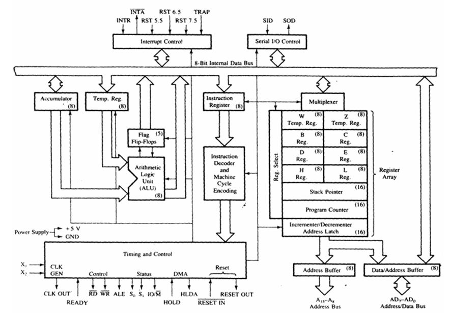
Fig:1.1 Architecture/block diagram of 8085 microprocessor
8085 Microprocessor Functional Units
The following are the functional units of 8085 microprocessor:
1. ALU (Arithmetic and logic unit)
ALU performs the following arithmetic and logical operations:
- Addition
- Subtraction
- Logical OR
- Logical AND
- Logical EXCLUSIVE OR
- Complement (Logical NOT)
- Increment (add 1)
- Decrement (subtract 1)
- Left shift, rotate left, rotate right
- Clear etc.
2. Timing and Control Unit
The timing and control unit is of the section of the CPU. It generates timing and control signal which are necessary for the execution of the instructions. It controls data flows between CPU and peripheral devices. it provides status, timing and control signals which are required for the operations of the memory and I/O devices.
3. Registers
As shown in the fig:1.1 here various registers of 8085. These registers are used by microprocessor for temporary data storage and manipulation of data and instructions. Data remain in the register till data send to the memory or I/O devices. Intel 8085 has the following registers:
- One 8-bit accumulator(ACC)
- Six 8-bit general purpose registers. These are B,C,D,E,H and L
- One 16-bit stack pointer (SP)
- One 16-bit program counter (PC)
- Instruction register
- Temporary register
8085 microprocessor consists additionally a set of five flip-flops which serves as flags which indicates some conditions which arise after the execution of arithmetic or logical instructions.
4. Accumulator (ACC)
The accumulator is an 8-bit register associated with the ALU. It is used to HOLD one of the operands of the arithmetic or logical operations. It serves as one input to the ALU. The other operands of the logical and arithmetic operations are stored either in memory or in any general-purpose register and the result finally stored in the ACCUMULATOR.
5. General purpose registers
8085 microprocessor contains 6, 8-bit general-purpose register. They are B, C, D, H and L registers. Here the combination of two 8-bit registers is known as register-pair.
The valid register pair in 8085 are: B-C, D-E, and H-L.
The programmer cannot make a pair as per his choice. The H-L pair is used as a memory pointer and for this purpose, it holds the 16-bit address of a memory location.
Advertisement
Advertisement