Home »
Embedded Systems
Pin diagram of 8255 PPI (Programmable peripheral interface)
In this tutorial, we will learn about the Pin diagram of the 8255 PPI (Programmable Peripheral Interface). We will study the complete IC structure of it, and will also study the functionalities that are performed by each of the pins.
By Monika Sharma Last updated : May 22, 2023
The following is the internal structure of the 8255 IC,
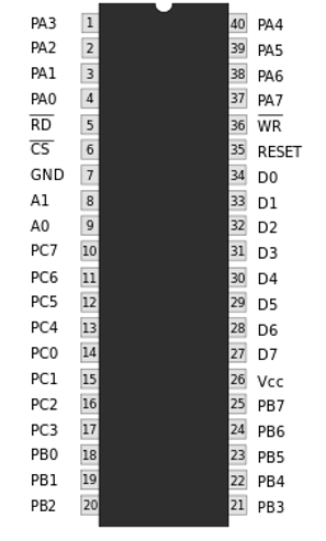
Image source: https://images.app.goo.gl/22BfM5mn9ZFo96S26
Let us take a look at the functionalities of each of its pins,
PA0 to PA1
These pins are the data lines for the port A. These pins are equally distributed on both sides of the top of the 8255 IC. The keys 1 to 4 and 37 to 40 are the pins devoted for port A.
PB0 to PB1
These pins are the data lines for Port B and the keys 18 to 25 are the pins that carry the data of port B.
PC0 to PC1
These pins are the data lines for the port C. The keys 10 to 17 carry the data bits of port A. Among these, the pins 10 to 13 are the Port C upper pins, and 314 to 17 are the pins devoted for port C lower.
D0 to D7
These pins carry the 8-bit binary code which is used to instruct the working of the entire IC. These pins together are called as the control word or control register. The keys 27 to 34 carry the contents of the control word.
A0 and A1
These pins decide which port will be selected for transferring the data. These keys are present at pins 8 and 9.
| A0 |
A1 |
Port selected |
| 0 | 0 | Port A |
| 0 | 1 | Port B |
| 1 | 0 | Port C |
| 1 | 1 | Control Register |
RD'
It is an active low signal key which puts the IC in reading mode. It is present at key number 5.
WR'
It is an active low signal key which puts the IC in writing mode. It is present at key number 36.
CS'
It is also an active low signal key which is responsible for chip selection. The key number 6 is devoted to chip select key.
RESET
This key present at 35 number when in set mode, resets the entire data present in all the keys to their default values.
GND
There is one ground key for 8255 IC present at key number 7.
VCC
The VCC key is from where the IC receives the 5V input. It is present at the key 26.
Advertisement
Advertisement